System Integration
Introduction
This section details the communication that occurrs between the FPGA and the MCU, accompanied by a system level blcok diagram and system level schematics.
It also details the many analog considerations we had to account for in order to properly transer signals between the FPGA, DAC, DUT, and MCU.
Communication between the FPGA and the MCU
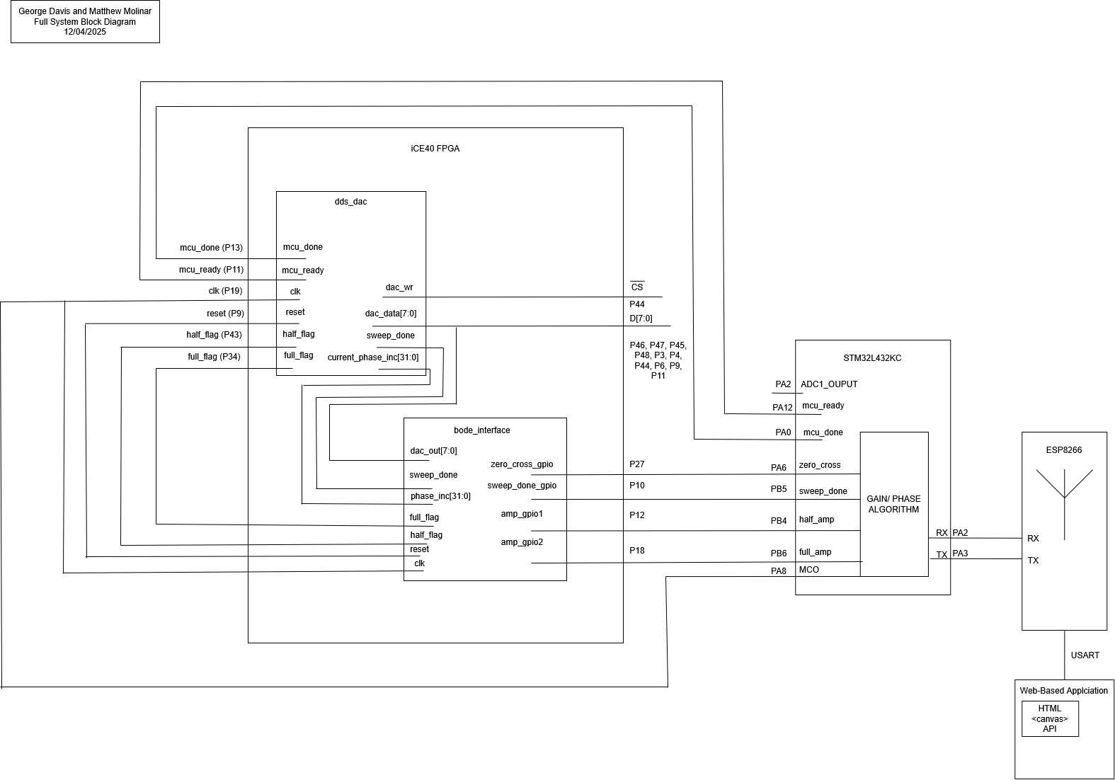
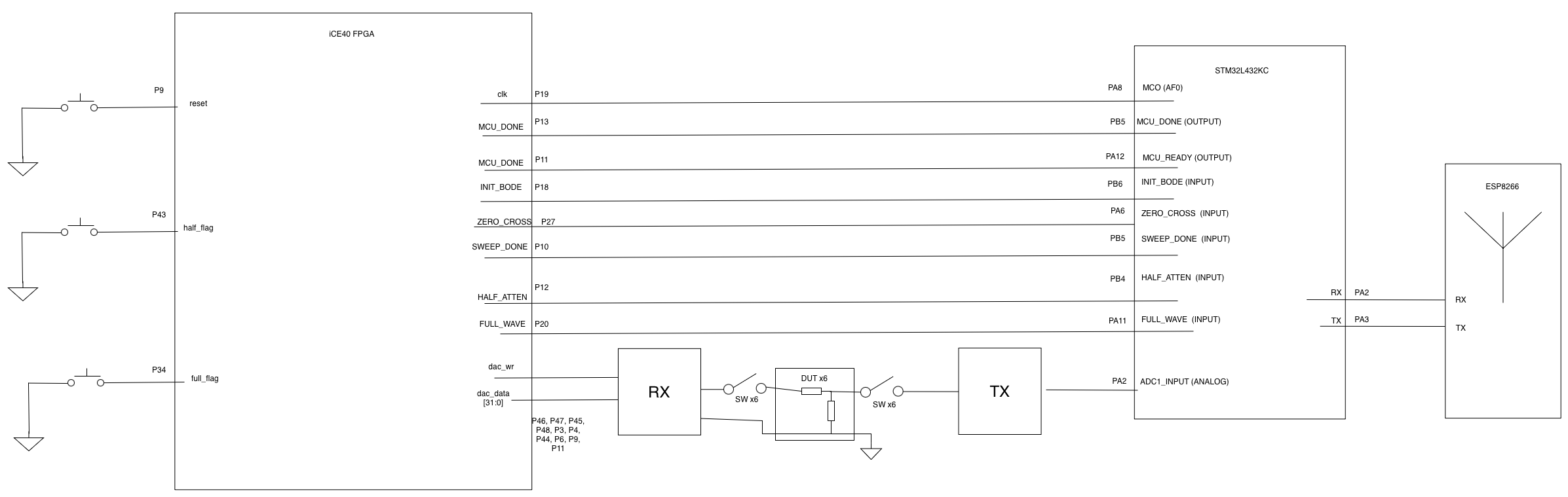
Our system is composed of an FPGA, an MCU, and an ESP8266. The FPGA is controlled by the MCU and is responsible for generating a sine wave frequency sweep from 100 Hz to 100 kHz. This frequency sweep drives an external DAC (AD5424), which outputs an analog signal that passes through a transmit chain, then a DUT (filter of choice), and through the receive chain. The MCU then uses its ADC peripheral to collect data throughout the frequency sweep in order to calculate the magnitude and phase responses as a result of the DUT. Finally, the MCU sends this data to an ESP8266 which hosts a webpage containing the bode plots that characterize the selected DUT.
System Block Diagram
System Schematics
External Hardware
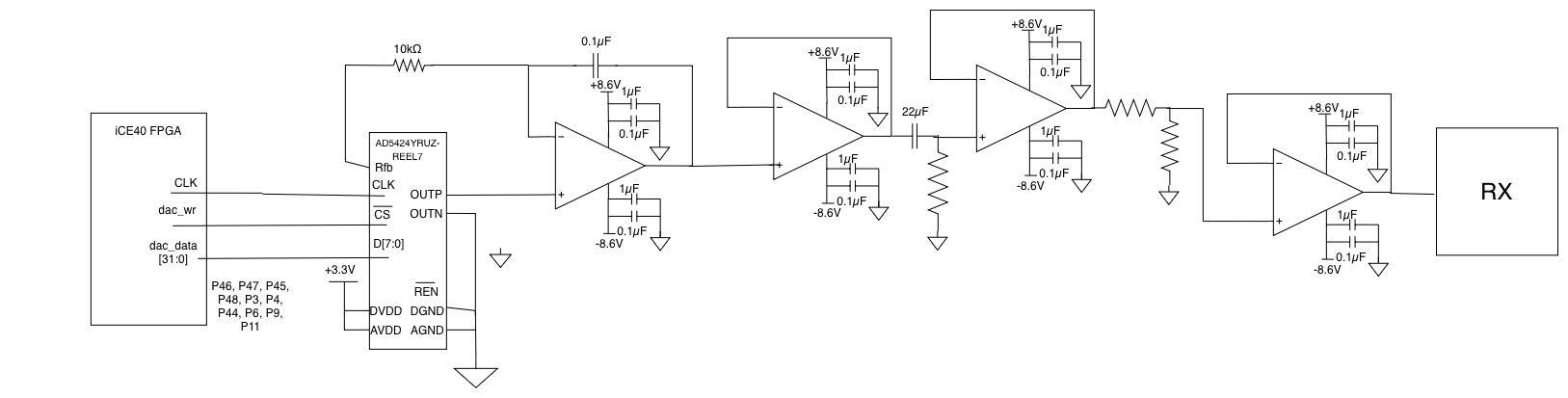
The new hardware we used was an AD5424, which is an 8-bit parallel DAC. We chose this DAC because it had a large update rate (20.4 MSPS) and a good multiplying bandwidth (10 MHz). The FPGA drives this DAC with parallel digital signals that represnt a sine wave, which is then converted into an anlog signal by the DAC. We needed this signal to be anlog so that it can be passed through our DUT and be picked up by the ADC thats onboard the MCU. This DAC is a current source which lead to a number of analog op amp considerations.
Analog Condiderations
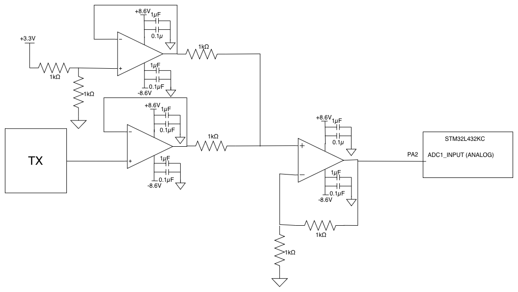
The primary analog considerations were noise reduction and op amp scaling to meet the input voltage range of the MCU. Two chains of op-amps were created using the TL084CN op-amp with a sufficient Gain Bandwidth Product of 5.25Mhz and a fast slew rate of 20V per microsecond.
The TX chain or transmit chain place the analog DAC output on a zero centered wave between -1.65 and 1.65 volts. We were able to do this accurately with a coupling circuit and inverting amplifier with gain. To limit noise we added decoupling capacitors to all op-amp rails. After we implemented this we saw a significant increase in our signal to noise ratio at large attenuation. Unity gain buffers were used liberally to ensure buffered impedance between sections of the circuit.
The RX chain needed to scale the received signal to the MCU input voltage range of 0 to 3.3V. We used a simple summing op amp with buffer to bring the wave from zero centered to the center of the input range.